Cluster PVD (Physical Vapour Deposition) systems have become an integral part of modern manufacturing processes. They offer precise and efficient deposition of thin films and coatings on various substrates, enabling the creation of cutting-edge products across a wide range of industries.
In this comprehensive guide, we will delve into the world of Cluster PVD systems, exploring their principles, applications, advantages, and the future of this technology.
What is Cluster PVD?
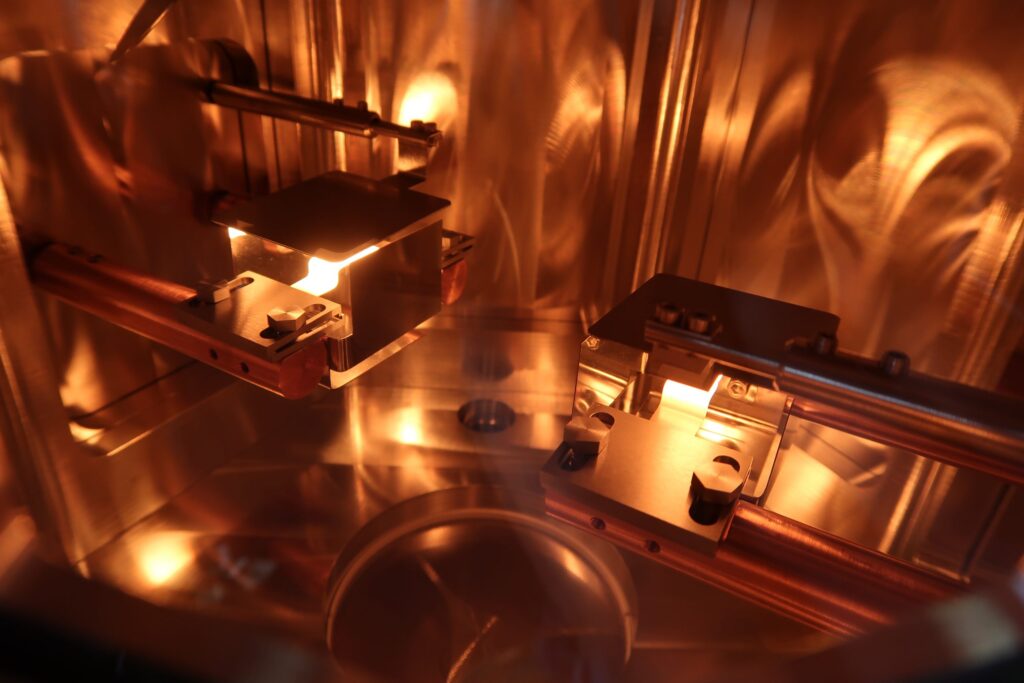
Source: korvustech.com
Cluster PVD is a specialised form of physical vapour deposition that involves the deposition of materials in clusters or nanoparticles rather than the traditional atomic or molecular scale. This technique employs a cluster source to generate clusters of atoms or molecules. Then, it deposits them onto a substrate. Cluster PVD can serve for both thin film deposition and surface modification.
The HEX-L Cluster from Korvus Technology offers a flexible and upgradable solution for Cluster PVD. Users can start with a single HEX-L chamber and later connect additional HEX-L chambers for in-vacuum sample transfer between them, providing a scalable and versatile platform for cluster deposition and surface modification.
How Cluster PVD Works
A Cluster PVD system operates by breaking down into several key steps:
- Cluster Generation: The first step involves generating clusters of atoms or molecules. Typically, technicians perform these processes using techniques such as gas aggregation or laser ablation.
- Cluster Acceleration: Once the clusters form, an electric or magnetic field accelerates them toward the substrate. This acceleration helps control the energy and direction of the cluster impact.
- Cluster Deposition: The accelerated clusters then deposit onto the substrate, adhering and forming a thin film or coating.
Applications of Cluster PVD
Cluster PVD systems find application in a wide range of industries, including:
- Electronics: Cluster PVD is used to deposit thin films for semiconductor devices, photovoltaic cells, and displays, enhancing their performance and durability.
- Optics: Manufacturers employ this technology in producing optical coatings, antireflection coatings, and reflective mirrors.
- Biomedical: Cluster PVD plays a crucial role in manufacturing bioactive coatings for medical implants, drug delivery systems, and diagnostic devices.
- Automotive: The automotive industry uses Cluster PVD for creating decorative and functional coatings on car parts, improving their wear resistance and corrosion protection.
- Aerospace: Aerospace applications include the deposition of thermal barrier coatings on turbine components and corrosion-resistant coatings on aircraft structures.
Advantages of Cluster PVD

Cluster PVD offers several distinct advantages over traditional deposition techniques. Its ability to deposit materials in the form of clusters or nanoparticles provides unique benefits in terms of control, efficiency, and performance. Here are some of the critical advantages of Cluster PVD:
- Precise Control: One of the most significant advantages of Cluster PVD is the ability to precisely control the size, composition, and structure of deposited clusters. This level of control allows for the creation of tailored thin films and coatings with specific properties.
- High Purity: Cluster sources can be designed to produce highly pure clusters, reducing the risk of contamination in the deposited films. This is especially important in industries like electronics and optics, where even trace impurities can impact performance.
- Reduced Waste: Cluster PVD is highly efficient, as it deposits material only where it’s needed, minimising material wastage. Traditional deposition methods may result in a significant amount of material loss during the process.
- Enhanced Adhesion: Clusters or nanoparticles tend to adhere better to substrates compared to individual atoms or molecules. This improved adhesion leads to coatings with better durability and adherence to the substrate.
- Customised Properties: Cluster PVD allows for the tailoring of material properties, including thickness, density, and morphology. This customisation is crucial in creating coatings with desired optical, electrical, or mechanical characteristics.
- Controlled Energy Impact: The energy of the clusters during deposition can be controlled and adjusted. This control is essential for influencing the properties of the thin film, such as its porosity, crystallinity, and stress levels.
- Uniformity: Cluster PVD can achieve excellent thickness uniformity across large substrates, ensuring consistent performance across the entire surface.
- Versatility: Cluster PVD can deposit a wide range of materials, including metals, semiconductors, insulators, and organic materials. This versatility makes it suitable for various applications and industries.
Future Trends in Cluster PVD
The field of Cluster PVD (Physical Vapour Deposition) continues to evolve, driven by advances in materials science, nanotechnology, and manufacturing processes. Here are some of the future trends and developments expected in Cluster PVD technology:
- Nanoscale Cluster Engineering: Researchers are exploring ways to engineer clusters at the nanoscale, allowing for precise control over cluster size, composition, and structure. This fine-tuning will enable the creation of materials with novel properties and functionalities.
- Eco-Friendly Cluster PVD: As sustainability becomes a top priority, there is a growing emphasis on developing environmentally friendly Cluster PVD processes. This includes reducing energy consumption, minimising waste generation, and using green precursor materials.
- Hybrid Deposition Techniques: Integration of Cluster PVD with other deposition techniques, such as chemical vapour deposition (CVD) and atomic layer deposition (ALD), is expected to increase. This synergy will provide more versatile material engineering options, allowing for the creation of complex multilayered structures.
- Advanced Materials for Electronics: Cluster PVD will continue to play a crucial role in the electronics industry, especially in the development of advanced materials for semiconductor devices, flexible electronics, and high-performance transistors.
- Energy Storage and Conversion: Cluster PVD will be used to deposit materials for energy storage applications, such as advanced battery materials (e.g., solid-state electrolytes) and materials for energy conversion (e.g., fuel cell catalysts).
- Biomedical Applications: Cluster PVD will be further utilised in the biomedical field to create specialised coatings for medical implants, drug delivery systems, and diagnostic devices. Research will focus on improving biocompatibility and controlled drug release.
- Optical and Photonics Advances: The optics and photonics industries will benefit from Cluster PVD advancements, particularly in the production of high-quality optical coatings, plasmonic materials, and advanced photonic devices.
- Aerospace and Automotive Industries: Cluster PVD will continue to enhance the performance and durability of components used in aerospace and automotive applications. This includes advanced coatings for turbine blades, lightweight materials, and corrosion-resistant coatings.
Final Thoughts
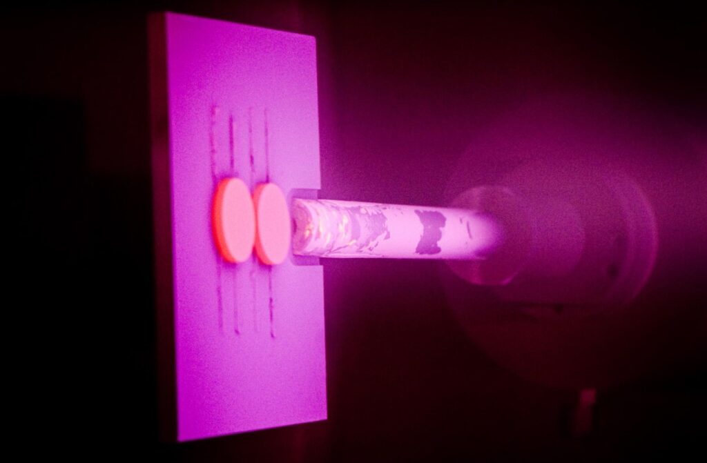
Source: en.wikipedia.org
Cluster PVD systems are revolutionizing the world of thin film deposition and surface modification. Their ability to create tailored coatings with enhanced properties makes them indispensable in various industries.
As technology advances, Cluster PVD is likely to continue evolving, offering even greater precision and versatility in material engineering. Understanding the principles and applications of Cluster PVD is essential for those looking to harness its potential for innovation and product development.


